Inside the Solar Cell: How the p–n Junction Converts Light into Electricity
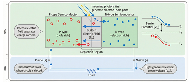
At the heart of every solar photovoltaic (PV) module lies a deceptively simple structure: the p–n junction. While solar installations may span hectares and generate gigawatts of power, their fundamental operation depends on microscopic processes occurring within semiconductor materials. Figure illustrates the photovoltaic effect in a p–n junction, the core mechanism by which sunlight is converted into usable electrical energy.
A solar cell is typically made from silicon, a semiconductor material whose electrical properties can be precisely controlled through a process known as doping. By introducing small amounts of specific impurities, silicon can be engineered into two distinct regions: p-type, rich in positive charge carriers (holes), and n-type, rich in negative charge carriers (electrons). When these two regions are brought together, they form a p–n junction.
At the interface of the p-type and n-type materials, an internal electric field is created. This field arises because electrons from the n-side diffuse into the p-side, while holes move in the opposite direction, until equilibrium is reached. The resulting region—called the depletion zone—is devoid of free charge carriers but contains a built-in electric field. This field is essential for photovoltaic operation.
When sunlight strikes the solar cell, photons with sufficient energy are absorbed by the silicon lattice. This energy excites electrons, allowing them to break free from their atomic bonds and form electron–hole pairs. In the absence of an electric field, these charge carriers would quickly recombine, releasing their energy as heat. The p–n junction prevents this from happening.
The internal electric field within the depletion zone drives electrons toward the n-type side and holes toward the p-type side. This separation of charge creates a voltage difference across the cell terminals. When an external circuit is connected, electrons flow through the circuit to recombine with holes on the p-side, producing a direct current. This is the photovoltaic effect in action.
Figure simplifies this process into a visual representation, showing photon absorption, carrier generation, charge separation, and current flow. While real solar cells incorporate additional layers—such as anti-reflective coatings, passivation layers, and metal contacts—the p–n junction remains the functional core.
The efficiency of this process depends on several factors. Band gap energy determines which photons can be absorbed; silicon’s band gap allows it to capture a significant portion of the solar spectrum, though not all of it. Photons with insufficient energy pass through the cell, while excess energy from higher-energy photons is lost as heat. This fundamental trade-off limits the maximum efficiency of single-junction silicon cells.
Recombination losses also play a critical role. Imperfections in the crystal structure, surface defects, and impurities can cause electrons and holes to recombine before contributing to useful current. Modern cell designs employ advanced passivation techniques to reduce these losses, improving both voltage and overall efficiency.
Temperature further influences p–n junction behavior. As temperature rises, the semiconductor’s electrical characteristics change, leading to reduced open-circuit voltage. This is why solar modules produce less power on very hot days, even under high irradiance.
Understanding the photovoltaic effect at the p–n junction level is essential for appreciating why certain technologies outperform others. Advanced architectures such as PERC, TOPCon, and heterojunction cells focus on improving charge separation, reducing recombination, and enhancing carrier collection—all refinements of the basic p–n junction concept.
Figure connects abstract semiconductor physics to real-world energy generation. It explains why material selection, cell design, and manufacturing precision matter, and why incremental improvements at the microscopic level can yield significant gains at the system scale.
In essence, every kilowatt-hour produced by a solar plant begins with this quiet, invisible process: photons striking a p–n junction and setting electrons in motion. Mastery of this fundamental mechanism underpins all progress in photovoltaic technology.
0 Comments