The Quantum Engine: Inside the Atomic Heart of a Solar Cell
We’ve looked at the full system architecture, and we’ve analyzed the geometry of the sun’s path. Now, it is time to zoom in—way in.
At the microscopic level, a solar panel isn’t just a slab of glass and metal. It is a precise “silicon sandwich” designed to trap light and force it to do work. This is the realm of Quantum Physics, where photons collide with electrons to create the Photovoltaic Effect.
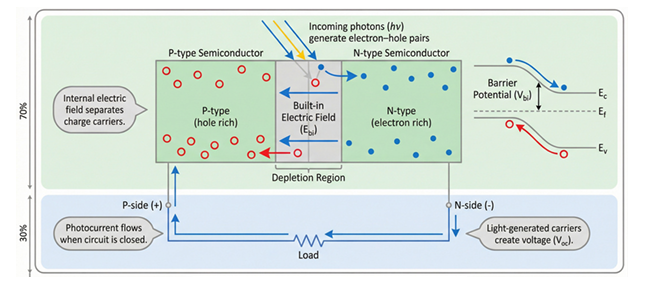
Based on the cross-sectional diagram provided, let’s deconstruct the atomic machinery that turns sunlight into electricity.
Part 1: The Setup – The P-N Junction
The diagram shows a block of semiconductor material divided into two distinct regions. This boundary is called the P-N Junction, and it is the most critical component of any solar cell.
1. The Ingredients (Doping)
Pure silicon acts as an insulator; it doesn’t conduct electricity well. To change this, manufacturers “dope” the silicon with impurities:
- N-type Semiconductor (Right Side): Doped with Phosphorus. This side is “Electron Rich” (represented by the blue dots). It has extra negatively charged electrons waiting to move.
- P-type Semiconductor (Left Side): Doped with Boron. This side is “Hole Rich” (represented by the red circles). “Holes” are simply the absence of an electron—spaces waiting to be filled.
2. The Depletion Region
Where these two materials touch, a fascinating reaction occurs. Some electrons from the N-side rush over to fill holes in the P-side. This creates a neutral zone in the middle called the Depletion Region (labeled in the center).
This movement creates a permanent Built-in Electric Field ($E_{bi}$). Think of this field as a one-way valve or a steep hill; it prevents electrons from flowing back unless they are given a massive push.
Part 2: The Spark – Photon Absorption
Now, we introduce sunlight. The diagram shows Incoming Photons ($h\nu$) striking the junction.
When a photon with enough energy hits a silicon atom in the Depletion Region, it knocks an electron loose from its bond.
- Electron-Hole Pairs: This collision creates two free carriers: a negatively charged Electron (blue) and a positively charged Hole (red).
Without the P-N junction, this electron would just fall back into the hole, and the energy would be lost as heat. But remember the “one-way valve” we created?
Part 3: The Separation – Internal Electric Field
This is where the magic happens.
- The Field separates the carriers: The internal electric field ($E_{bi}$) instantly pushes the free Electron to the N-side and the Hole to the P-side.
- The Energy Band Diagram: The right side of the image illustrates this energetically. The electron is “excited” from the Valence Band ($E_v$) up to the Conduction Band ($E_c$).
- The Barrier Potential: Once up there, the “slope” of the energy bands slides the electron down to the N-side. It is now trapped on that side of the fence.
As millions of photons hit the cell every second, the N-side becomes packed with electrons, and the P-side becomes packed with holes. This charge imbalance creates voltage ($V_{oc}$ or Open Circuit Voltage).
Part 4: The Flow – Powering the Load
The electrons on the N-side are desperate to get back to the holes on the P-side to recombine. But the internal field prevents them from crossing the junction directly.
We give them an alternative path: The External Circuit (The bottom 30% of the diagram).
- We connect a wire to the N-side (-).
- The electrons flow out of the cell, through the wire, and pass through a Load (a lightbulb, a battery, or the grid).
- As they pass through the load, they do work (lighting the bulb).
- They return to the P-side (+) and finally recombine with a hole.
This flow of electrons is what we call Direct Current (DC) electricity.
Why Efficiency Matters
This diagram also hints at why solar panels aren’t 100% efficient.
- Band Gap: If a photon has too little energy (low $h\nu$), it can’t knock the electron up to the Conduction Band ($E_c$). It passes right through the cell.
- Recombination: Sometimes, an electron falls back into a hole before the field can separate them. This is wasted energy.
By understanding the physics of the P-N Junction, engineers can tweak materials and doping levels to catch more photons and reduce losses, pushing the limits of modern solar technology.
0 Comments